Knowledge
Manual Zoom Lens for Semiconductor and Microelectronics Observation
Semiconductor observation splits into two jobs that are often confused. One is production inspection, where magnification is changed by a machine inside a recipe. The other is engineering observation — failure analysis, first-article review, process development, incoming die checks — where an engineer changes magnification by hand while looking at the same device. A manual zoom lens is the correct instrument for the second job and the wrong one for the first. This article sets out the optical requirements of engineering observation, what the POMEAS 14× class actually delivers, and where a zoom lens stops being a valid instrument.
Why engineering observation is a different problem
Production inspection measures a defined feature at a defined magnification, thousands of times, and needs repeatability above all. Engineering observation is exploratory: the engineer does not yet know which feature matters, so the view has to move from a whole die to a single bond wire without losing orientation. That is a human-in-the-loop task, and the interface that suits it is a ring, not a recipe.
Three consequences follow. The zoom range has to be wide enough that the engineer never has to remount the lens mid-observation. The working distance has to clear whatever probe, probe card or fixture is in the way. And the image has to be bright enough at every setting to be judged, because an observation that requires a 500 ms exposure is an observation that cannot be made while adjusting a probe.
What the 14× class delivers
The POMEAS 14× continuous zoom lens, PMS-LZH-14105K, is specified at 0.55× to 7.6× optical magnification with a 14:1 zoom ratio, 77.8 ± 2 mm working distance, a 2/3-inch maximum sensor and a C-mount interface. Published optical resolution improves from 14.59 µm at 0.55× to 2.80 µm at 5× and above, and coaxial illumination is available.
Those resolution figures are the honest limit of the instrument. At 2.80 µm, a 1 µm feature cannot be resolved no matter what camera is attached — it will be visible as a blur of about three resolution widths, which is enough to notice that something is there and not enough to measure it. Saying so up front prevents the most common disappointment with zoom optics in semiconductor work.
| Magnification | FOV on 1/3″ | FOV on 1/2″ | FOV on 2/3″ | Resolution | DOF |
|---|---|---|---|---|---|
| 0.55× | 8.73 × 6.55 mm | 11.64 × 8.73 mm | 16.00 × 12.00 mm | 14.59 µm | 3.16 mm |
| 1× | 4.80 × 3.60 mm | 6.40 × 4.80 mm | 8.80 × 6.60 mm | 8.18 µm | 0.98 mm |
| 2× | 2.40 × 1.80 mm | 3.20 × 2.40 mm | 4.40 × 3.30 mm | 4.30 µm | 0.26 mm |
| 3× | 1.60 × 1.20 mm | 2.13 × 1.60 mm | 2.93 × 2.20 mm | 3.49 µm | 0.14 mm |
| 4× | 1.20 × 0.90 mm | 1.60 × 1.20 mm | 2.20 × 1.65 mm | 3.05 µm | 0.09 mm |
| 5× | 0.96 × 0.72 mm | 1.28 × 0.96 mm | 1.76 × 1.32 mm | 2.80 µm | 0.07 mm |
| 7× | 0.69 × 0.51 mm | 0.91 × 0.69 mm | 1.26 × 0.95 mm | 2.80 µm | 0.05 mm |
These are manufacturer specifications for the lens, not measurements made for this article. The fields are object-side and assume the sensor format in the column header.
Matching a camera to the resolution limit, not to a megapixel number
At 7× on a 2/3-inch sensor the field is 1.26 mm wide. A 1920-pixel camera samples that at 0.82 µm per pixel, which is already 3.4 times finer than the 2.80 µm optical resolution. Sampling finer than the optics can deliver buys nothing: the image gets bigger without getting sharper. A 5-megapixel 2/3-inch camera at 2448 pixels samples 0.64 µm per pixel, roughly 4.4 times finer than the optical limit, which is already beyond the useful point.
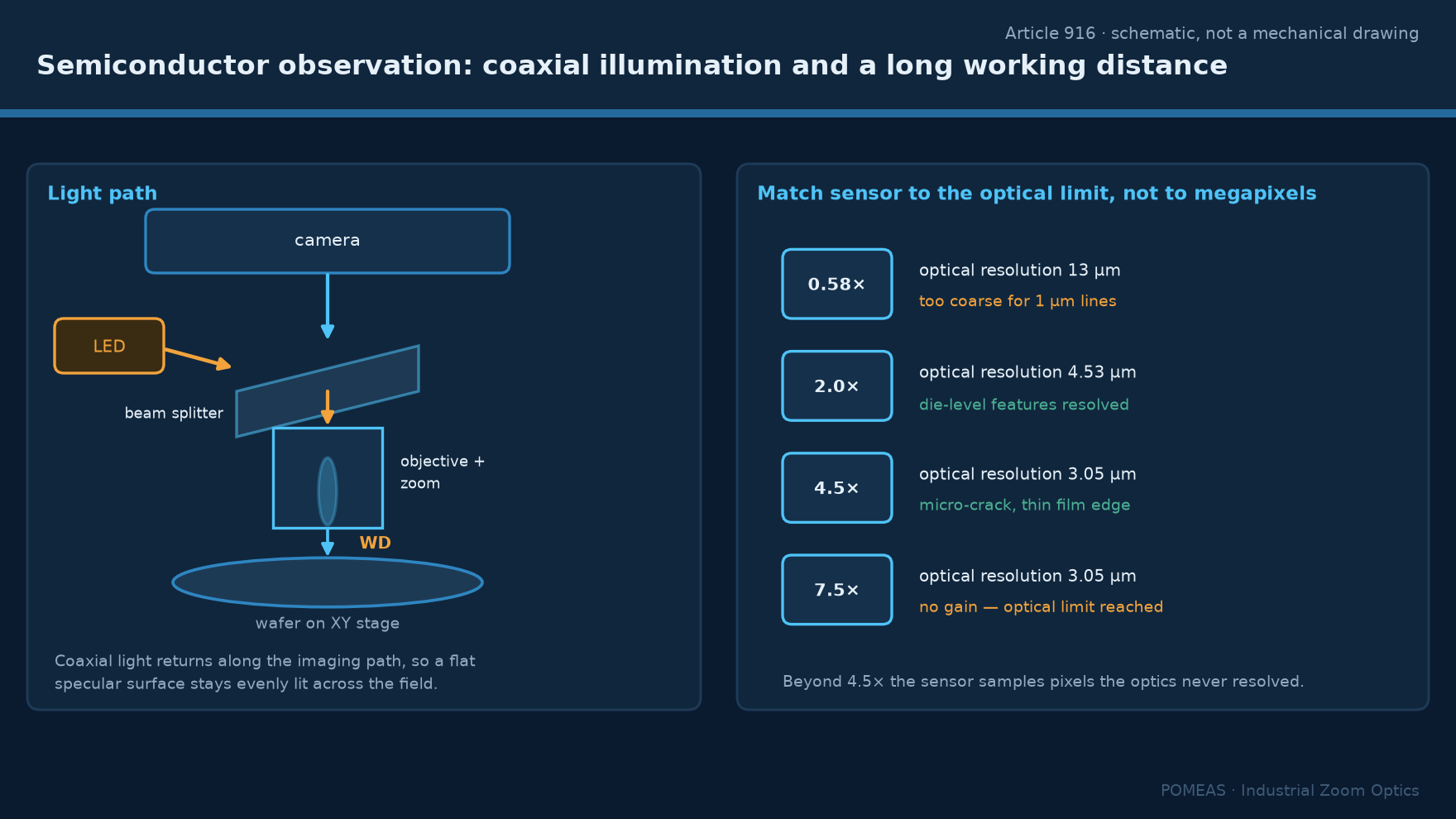
The practical conclusion for engineering observation is that a 2 to 5 megapixel camera is sufficient with this lens, and money is better spent on illumination and on a stable mount than on more pixels. The general rule that sampling should be about three pixels per resolvable feature is derived in magnification is not resolution.
What "2000×" means, and why it is not comparable
Microscope vendors quote total visual magnification, which is objective magnification times eyepiece magnification. A 100× objective with a 20× eyepiece is quoted as 2000×, and that number has no direct equivalent in a camera system, because the camera replaces the eyepiece and the display replaces the eye. What carries over is the object-side field: a 100× objective on a standard tube has a field of about 0.2 mm, and to get a 0.2 mm field on a 2/3-inch sensor you need 8.8 ÷ 0.2 = 44×, which is beyond a 14× zoom lens.
This is why a zoom lens is not a replacement for a high-power objective. It covers the 0.55× to 7.6× band, which corresponds to object fields from 20 mm down to about 1.2 mm on a 2/3-inch sensor. Beyond that, a dedicated objective on a microscope body or an electron microscope takes over. The conversion arithmetic between the two conventions is set out in microscope to machine vision: camera, lens and magnification.
Where a zoom lens is genuinely better than a microscope body
Three situations. First, when the sample sits inside a probe station or a handler and cannot be brought to a microscope: the lens goes to the sample on a bracket, and 77.8 mm of working distance is enough to clear most probes. Second, when several engineers need to see the same view during a discussion: a screen is shareable and an eyepiece is not. Third, when the observation has to be recorded with the magnification visible in the frame, which a captured image with a scale does and an eyepiece view does not.
A fourth, less obvious advantage: a C-mount zoom lens mounts on the same camera and the same software as the rest of the vision system, so an engineering observation can use the same capture and annotation tools as production images.
Illumination is the limiting factor more often than the lens
At 5× and above, the illuminated area is about 2 mm across. Coaxial illumination through the lens is the standard answer for flat, reflective specimens such as a die surface or a polished cross-section, because it puts light on the optical axis and returns specular reflection straight back. It is the wrong answer for a bond wire loop, where the wire's curvature sends light away from the axis and the wire reads as a dark line against a bright field — which is often exactly what is wanted, but it means the illumination choice follows the feature, not the lens.
For transparent layers and coatings, coaxial light produces interference fringes that can be mistaken for surface structure. If that matters, the setup needs crossed polarisers or oblique illumination, and the observation should be described as qualitative.
Where a zoom lens stops being valid
A zoom lens is not a metrology instrument. It has no calibrated magnification readout in the manual version, its distortion changes with zoom position, and its depth of field at high magnification is a few tens of micrometres. Any dimensional claim — line width, bump height, die placement — requires either a telecentric system with a calibrated scale or a dedicated measuring instrument. The distinction between a lens that shows a feature and a system that measures it is the subject of industrial microscope versus zoom microscope system.
Nor does a zoom lens belong inside a production loop where magnification is switched per part. That is a motorised application, and the requirements are different: position feedback, repeatable detents, and a control interface. Those are covered in motorised zoom plus APO for semiconductor wafer inspection.
Frequently asked questions
Can a 7.6× zoom lens see a 1 µm feature?
No. The published optical resolution at high magnification is 2.80 µm, so a 1 µm feature falls below the diffraction limit of the instrument and appears as a soft spot rather than a defined shape. Seeing it requires a higher-NA objective, not a higher-magnification zoom setting.
Is coaxial illumination necessary for wafer observation?
For a planar, reflective surface such as an unpatterned die or a polished cross-section, coaxial illumination gives the most even result and is usually the right default. For patterned layers with transparent films it can produce interference artefacts, in which case oblique or polarised light is better.
Why does the image get dark when I zoom in?
Because the effective f-number rises with magnification: the same aperture admits less light per unit image area as the lens groups move. Expect roughly a six-fold drop in illumination across a 12.5× range. Increase light output or exposure rather than assuming the lens is faulty.
Can I use this lens for die attach inspection on a production line?
Only if the magnification is fixed for the recipe. A manual lens cannot report its position, so a production record cannot state at what magnification an image was taken. For a line application, the motorised variant of the same optics is the correct choice.
What sensor format should I pair with a 14× lens?
2/3-inch is the maximum supported. A smaller sensor crops the field and gives a narrower view at the same magnification; a larger sensor will vignette. If a wider field is needed at low magnification, a 1-inch 4K zoom lens covers 18.8 mm at 0.68×, wider than this lens at 0.55×.
How stable does the mount need to be?
At 7× the field is 1.26 mm on a 2/3-inch sensor, so a 10 µm vibration moves the image by roughly 0.6 percent of the frame — visible as blur at short exposures. A rigid bracket and a damped bench matter more at high magnification than at low.

Subscribe to Our Newsletter
Simply enter your email to receive the latest news and insights from Pomeas. Stay connected with Pomeas and be the first to discover new innovations in optical excellence.