Machine Vision Zoom Lenses for Electronics & Semiconductor Inspection
In electronics manufacturing and semiconductor inspection, one common imaging challenge is the need to combine a relatively large field of view for fast target location with higher magnification for observing small details such as solder joints, chip edges, connector pins, bonding wires, and adhesive edges.
The main advantage of an industrial continuous zoom lens is its ability to continuously change optical magnification within the same imaging system, allowing users to switch from overall target positioning to detailed local inspection without frequently replacing the lens. For applications that require flexible switching between a large field of view and detailed observation, the POMEAS 6.5X continuous zoom lens can be considered.
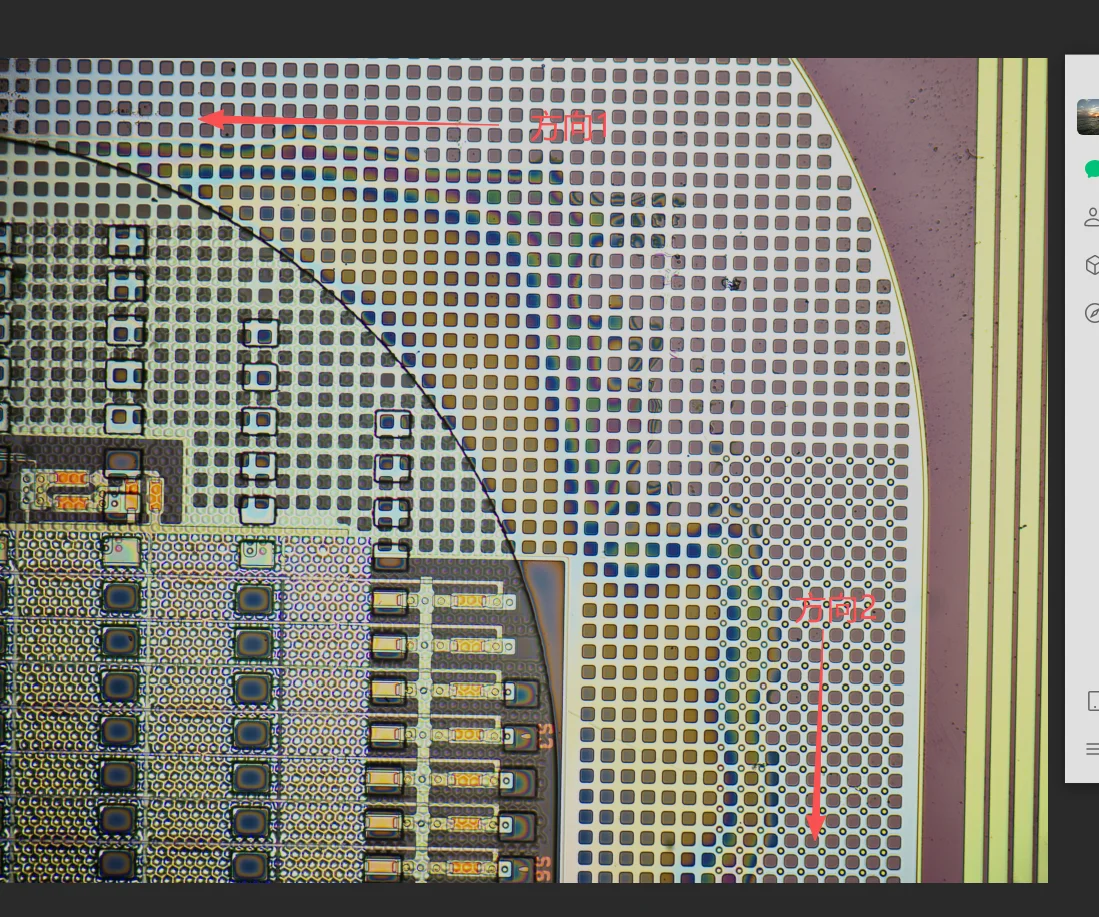
What Can a Machine Vision Zoom Lens Inspect in Electronics Manufacturing?
In electronics and semiconductor manufacturing, zoom lenses are not limited to one specific type of product. Whenever an inspection task requires switching between a larger field of view and higher-magnification local observation, a continuous zoom optical system may be suitable.
| Inspection Target | Typical Observation Tasks | Role of the Zoom Lens |
|---|---|---|
| PCB | Components, solder joints, contamination, scratches, missing parts | Locate the target first, then zoom into local details |
| Solder Joints | Insufficient solder, excess solder, solder bridging, surface condition | Higher magnification for small soldering areas |
| IC Chips | Surface defects, markings, edge chipping, particles | Observe the complete chip and local defects |
| Semiconductor Die | Edges, scratches, chipping, contamination | Switch quickly between different fields of view |
| Bonding Wire | Wire position, bonding points, deformation, broken wires | Magnify small connection areas |
| Connectors | Pins, bending, burrs, contamination | Inspect both complete pin arrays and individual pins |
| FPC | Circuit traces, scratches, broken traces, foreign particles | Observe the overall circuit and local structures |
| LED / Mini LED | Chip, electrodes, package, surface defects | Adapt to electronic components of different sizes |
| Glue / Adhesive | Overflow, missing glue, discontinuity, bubbles, glue width | Observe the complete glue path and zoom into edge details |
1. PCB Inspection
PCB inspection is one of the most common applications for industrial zoom lenses. A PCB may contain millimeter-scale components together with much smaller solder joints, circuit traces and surface defects. A single fixed field of view may therefore be unable to provide both efficient target location and detailed observation.
Typical PCB inspection tasks include:
- Missing or misaligned electronic components
- PCB solder joint condition
- Solder bridging
- Insufficient or excess solder
- Scratches on circuit traces
- PCB surface contamination
- Pad surface condition
- Component markings and characters
With a zoom lens, users can first locate the target at lower magnification and then increase magnification to inspect an individual solder joint, pad or component edge. This combination of large-field target location and high-magnification local inspection is one of the main advantages of continuous zoom lenses in electronics inspection.
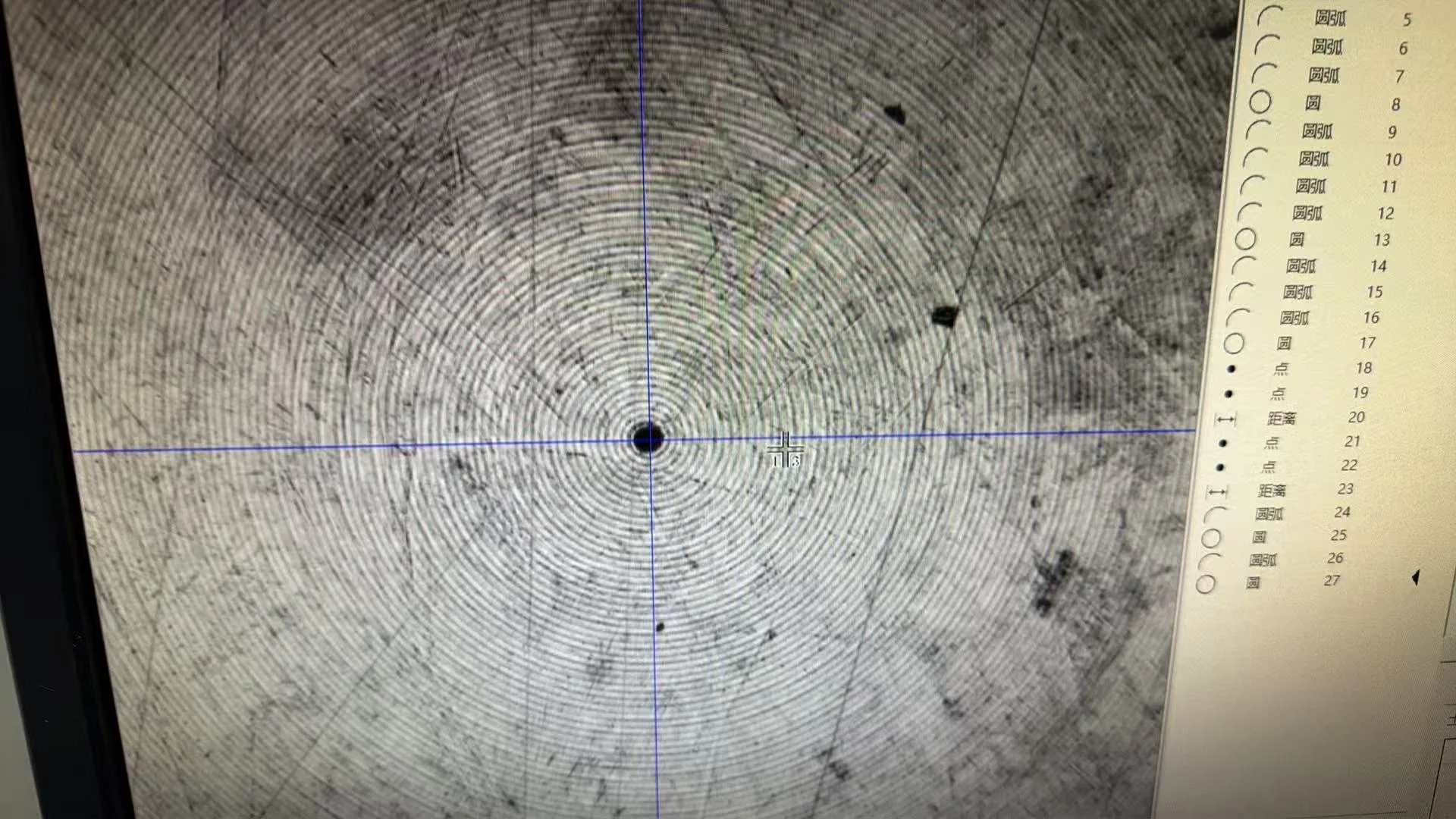
2. PCB Solder Joint Inspection
PCB solder joints are usually small and highly reflective. For this reason, image quality depends not only on lens magnification but also heavily on the illumination method.
Typical solder joint inspection tasks include:
- Insufficient solder
- Excess solder
- Solder bridging
- Abnormal solder joint shape
- Surface contamination
- Local cracks
- Foreign particles around the soldering area
What Lighting Is Suitable for Solder Joint Inspection?
Solder is a reflective material, so there is no single lighting method that works for every solder joint. Common options include ring lights, coaxial illumination, low-angle lighting and diffuse illumination. The final lighting method should be selected according to solder joint geometry, surface reflectivity and the defect that needs to be highlighted.
3. IC Chip & Semiconductor Die Inspection
IC chip and semiconductor die inspection often requires switching between the complete device and a very small local area. For example, the operator may first inspect the overall chip position and outline, and then zoom into one corner to check for edge chipping, scratches or particle contamination.
Typical inspection targets include:
- Chip surface scratches
- Die edge chipping
- Particles and foreign materials
- Chip markings
- Electrode areas
- Package surface condition
- Local contamination
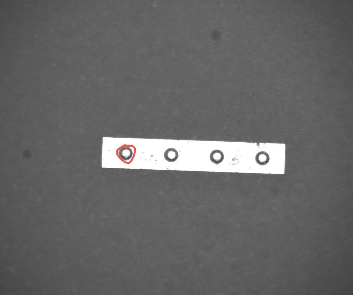
Is Higher Magnification Always Better?
No. As the target becomes smaller, the ability to clearly resolve details depends on the resolution of the complete optical system, not simply on the display magnification.
For very small semiconductor structures, lens NA, optical resolution, camera pixel size and actual field of view should all be considered. If the resolution of a standard zoom lens is insufficient, a high-NA objective or dedicated microscopic imaging system may be required.
For applications requiring higher optical resolution and support for larger camera sensors, the POMEAS 4K industrial zoom lens series can also be considered.
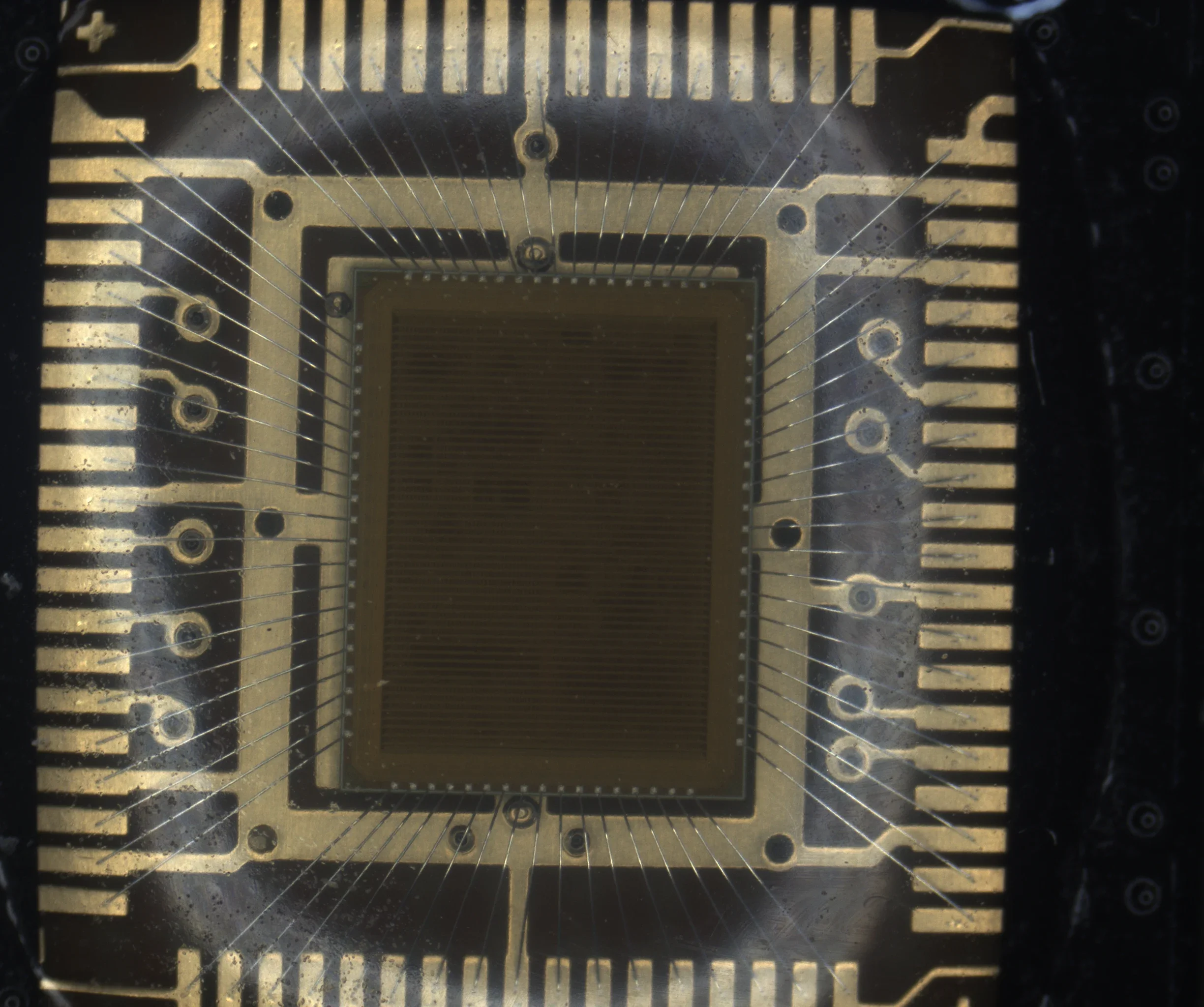
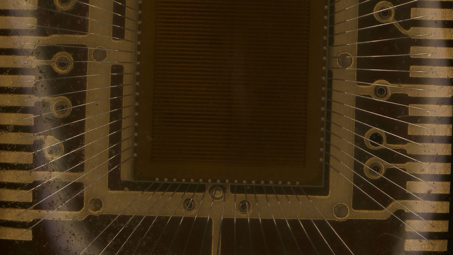
Real image: a QFP package captured at low magnification, leads and die both visible.
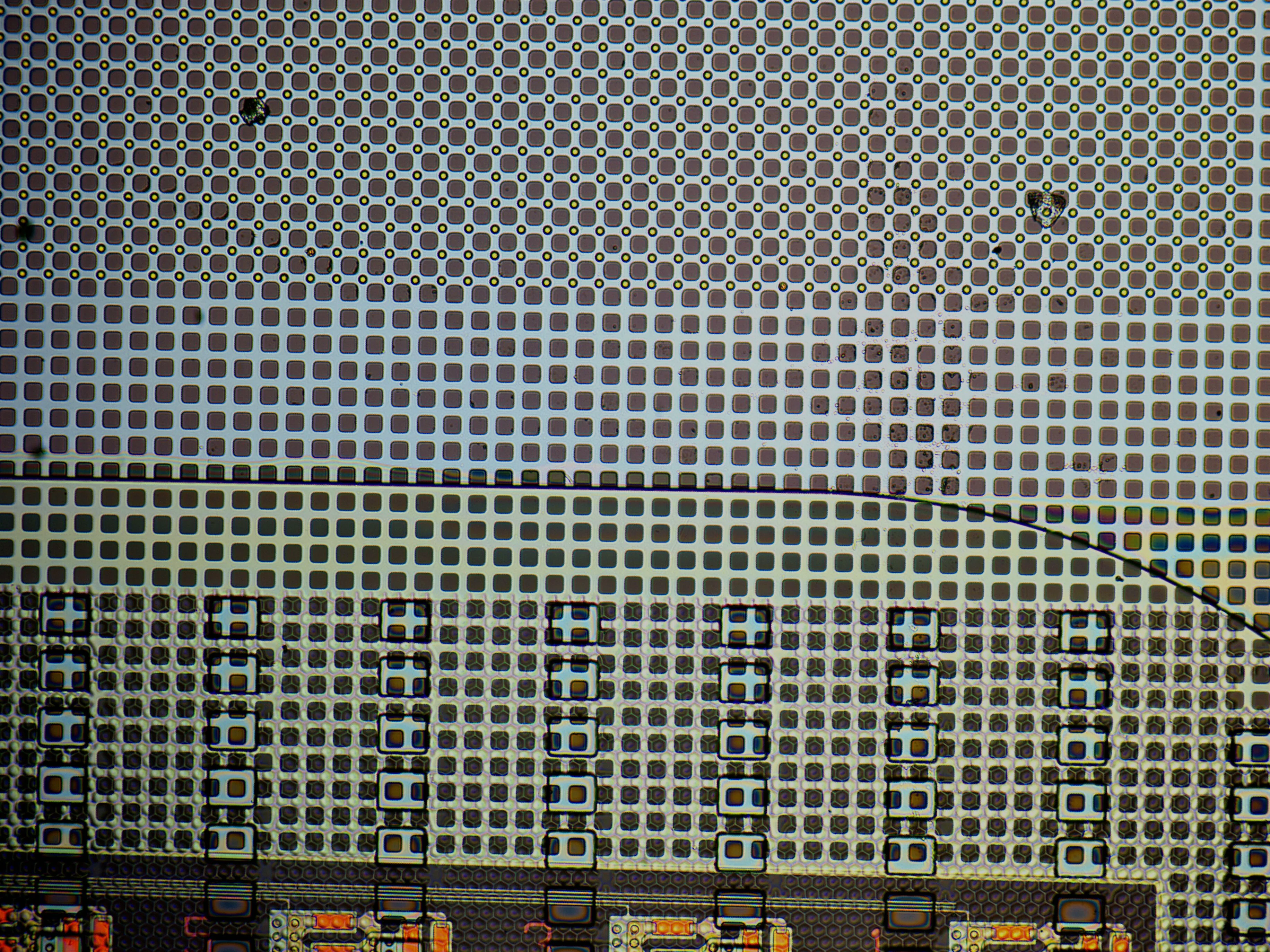
Real image: zooming in resolves the die surface and bonding region for defect review.
4. Bonding Wire Inspection
Bonding wires are typically very small and have reflective metallic surfaces. Inspection may involve not only the wire itself, but also bonding points and the surrounding connection area.
Typical observation tasks include:
- Bonding wire position
- Wire deformation
- Broken wires
- Connection areas
- Bonding point appearance
- Foreign particles and contamination
For reflective metallic structures, coaxial illumination, ring lighting or directional illumination can be tested according to the actual surface condition to improve contrast between the target and background.
5. BGA & Solder Ball Inspection
BGA components contain arrays of small solder balls. Visible-light zoom imaging systems can be used to inspect solder balls that are directly visible, as well as the package surface and surrounding structures.
Typical visible inspection tasks include:
- Solder ball position
- Missing solder balls
- Surface contamination
- Solder ball shape
- Mechanical damage
- Package surface defects
It is important to note that if the solder joints are hidden beneath an opaque BGA package, a conventional visible-light lens cannot directly inspect the internal structure. Other inspection technologies are required for internal BGA solder joint analysis.
6. Connector & Connector Pin Inspection
Connectors are widely used in consumer electronics, automotive electronics, communication equipment and industrial control systems. A typical connector inspection requirement is to observe the complete pin array and then zoom into one individual pin for detailed inspection.
Typical observation tasks include:
- Bent pins
- Missing pins
- Pin surface defects
- Burrs
- Contamination
- Terminal deformation
- Scratches
- Plating defects
What Is the Difference Between Observing and Measuring Connector Pins?
If the goal is simply to determine whether a pin has burrs, bending or surface damage, a zoom lens usually provides good flexibility.
However, if the application requires high-accuracy measurement of pin width, spacing or position, a telecentric lens should be considered to reduce perspective error and measurement variation caused by changes in object height.
7. FPC Flexible Printed Circuit Inspection
Flexible printed circuits often combine fine conductive traces with a relatively large overall size, making variable-field imaging useful for both complete-circuit observation and local defect inspection.
Typical inspection targets include:
- Circuit patterns
- Broken traces
- Scratches
- Surface contamination
- Foreign particles
- Connector areas
- Characters and markings
8. LED & Mini LED Inspection
Industrial zoom lenses can also be used for visual inspection of LEDs, Mini LEDs and other small electronic components.
Typical targets include:
- LED chips
- Electrodes
- Package structures
- Surface cracks
- Edge chipping
- Contamination
- Component position
As component dimensions become smaller, the match between optical resolution and camera pixel size becomes increasingly important. Simply increasing digital display magnification does not provide additional optical detail.
9. Glue, Adhesive & Dispensing Inspection
Glue and adhesive dispensing are also common machine vision applications in electronics manufacturing. Adhesives may be used for chip packaging, PCB assembly, camera modules, LED packaging, component fixation and electronic product sealing.
Typical dispensing defects include:
- Missing glue
- Broken or discontinuous glue lines
- Glue overflow
- Incorrect dispensing position
- Uneven glue width
- Bubbles
- Foreign particles
- Irregular adhesive edges
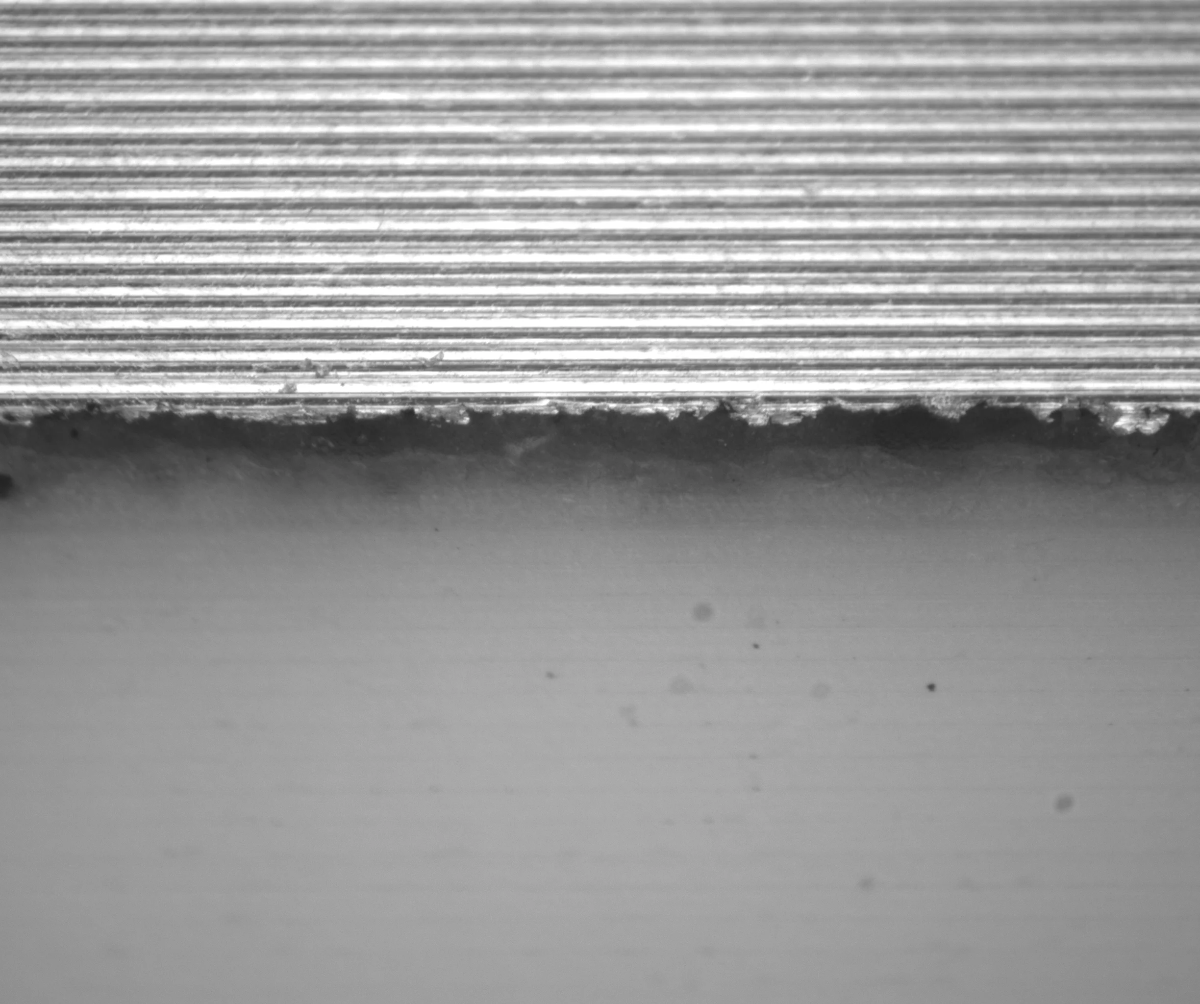
Can a Zoom Lens Inspect Transparent Adhesive?
Yes, but transparent adhesive is often not a problem of insufficient magnification. The real challenge is usually the lack of image contrast between the adhesive and the background.
For transparent glue, UV adhesive or transparent substrates, backlighting, low-angle illumination, dark-field lighting, polarization or other illumination methods may need to be tested to create sufficient grayscale contrast between the adhesive edge and the substrate.
Why Are Continuous Zoom Lenses Suitable for Electronics Inspection?
The real value of a continuous zoom lens is not simply to make an object appear larger. Its main advantage is the ability to provide different fields of view within the same imaging system.
A typical inspection workflow is:
Locate Target → Adjust Magnification → Zoom Into Local Area → Focus → Inspect Defect
This makes continuous zoom lenses particularly suitable for:
- Manual visual inspection stations
- Electronics repair and rework
- Failure analysis
- R&D laboratories
- Flexible automation equipment
- Multi-model product inspection
- Machine integration requiring multiple magnifications
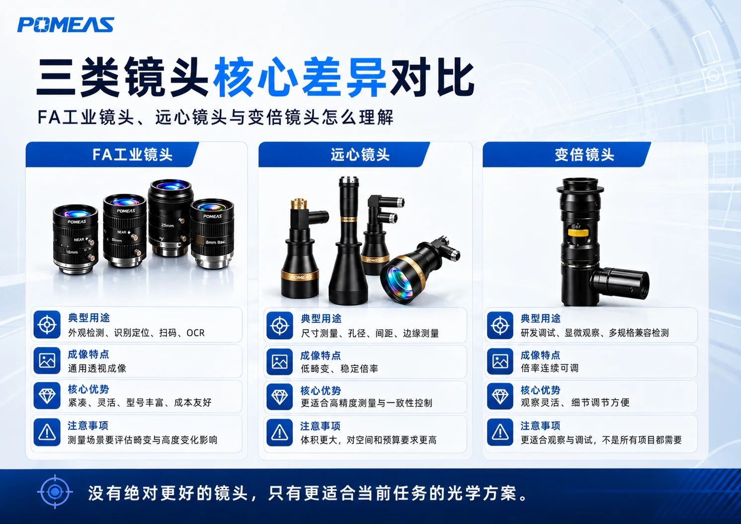
To explore additional machine vision lenses and related imaging products, visit the POMEAS Machine Vision Product Center .
6.5X vs 12.5X Zoom Lens: Which One Should You Choose?
6.5X Continuous Zoom Lens
For PCB, solder joint, connector and general electronic component inspection, if the difference between the largest required field of view and the smallest field of view is moderate, a 6.5X continuous zoom lens can usually provide sufficient flexibility.
12.5X Continuous Zoom Lens
If the same imaging system needs both a relatively large overview and significantly higher magnification for detailed observation, a larger zoom ratio provides a wider usable magnification range.
For automated equipment requiring motorized magnification adjustment, coaxial illumination and a wider zoom range, the 12.5X motorized coaxial zoom lens can be considered.
However, lens selection should not be based only on whether the lens is 6.5X or 12.5X. The camera sensor size, required field of view, smallest defect, working distance and installation space should also be confirmed.
How Should an Industrial Camera Be Matched with a Zoom Lens?
The camera and lens should be selected as one complete imaging system.
Important parameters include:
- Camera sensor size
- Camera resolution
- Pixel size
- Required field of view (FOV)
- Smallest feature that must be resolved
A higher camera pixel count provides more sampling points within the same field of view, but this does not mean that simply replacing the camera with a higher-megapixel model will automatically reveal smaller defects.
If the optical system cannot resolve the required detail, increasing the camera resolution alone will not provide more useful optical information. For this reason, lens resolution, camera pixel size and object-side field of view should be evaluated together.
How to Select Lighting for Electronics Inspection
| Inspection Target | Possible Lighting Method |
|---|---|
| General PCB | Ring light |
| Flat reflective metal surfaces | Coaxial illumination |
| Scratches and edge defects | Low-angle / dark-field illumination |
| Profiles and silhouettes | Backlight |
| Highly reflective components | Diffuse illumination |
| Glue and transparent materials | Lighting should be tested according to the adhesive and substrate |
Lighting should therefore not be selected simply because the application belongs to the electronics industry. More important factors include surface material, reflectivity, geometry and the defect that needs to be highlighted.
When Should You Use a Zoom Lens and When Should You Use a Telecentric Lens?
A Zoom Lens Is More Suitable When:
- Magnification needs to be changed
- Both overall observation and local magnification are required
- The same equipment must inspect products of different sizes
- The main goal is visual defect inspection rather than high-accuracy dimensional measurement
- High system flexibility is required
A Telecentric Lens Should Be Considered When:
- High-accuracy dimensional measurement is required
- Perspective error must be minimized
- The object has height variation
- Stable magnification is required
- Highly repeatable geometric measurement is needed
For example, if the purpose is simply to determine whether a connector pin has a burr, a zoom lens provides excellent flexibility.
However, if the application requires high-accuracy measurement of pin width, spacing or position, a C-Mount telecentric lens should be further evaluated.
What Information Is Needed to Select the Right Zoom Lens?
For PCB, chip, semiconductor, connector, LED or adhesive inspection, providing the following information can help determine a suitable lens and camera configuration more quickly:
- What product will be inspected? PCB, chip, solder joint, connector, adhesive, etc.
- What needs to be observed? Scratch, burr, edge chipping, bubble, missing glue or another defect.
- What field of view is required? For example, 20 × 15 mm or 4 × 3 mm.
- What is the smallest feature that must be clearly visible? For example, 0.1 mm, 50 μm or 10 μm.
- What industrial camera is being used? Including sensor size, resolution and pixel size.
- What working distance is available?
- What is the surface material? Reflective metal, PCB, transparent adhesive, glass or plastic.
- Is the main purpose observation or dimensional measurement?
For machine vision lens selection, field of view, smallest feature size and camera parameters are usually more meaningful than simply requesting a certain display magnification.
Need Help Selecting an Optical Configuration?
Provide the camera model, field of view, working distance, sample size and smallest feature that must be observed. POMEAS can help evaluate a suitable zoom lens, industrial camera and lighting configuration.
Frequently Asked Questions
Can an industrial zoom lens inspect PCB solder joints?
Yes. Continuous zoom lenses can be used to observe solder joint shape, solder bridging, insufficient solder, excess solder and other visible surface conditions. Because solder surfaces are reflective, appropriate lighting is also important for obtaining sufficient image contrast.
Can a zoom lens be used for semiconductor chip inspection?
Yes. It can be used for chip surface inspection, edge observation, markings, particles, contamination and local defect inspection. If extremely small semiconductor structures must be resolved, lens NA and optical resolution should be evaluated carefully.
Can a zoom lens inspect glue and adhesive dispensing defects?
Yes. Visible defects such as missing glue, discontinuous glue, overflow, bubbles and adhesive edge condition can be observed. For transparent adhesives, lighting is often more important than simply increasing magnification.
Is higher magnification always better?
No. As magnification increases, the field of view usually becomes smaller, and depth of field also changes. Magnification should be selected according to the required field of view and the smallest feature that must actually be resolved.
Does PCB inspection require coaxial illumination?
Not always. Coaxial illumination is suitable for certain flat reflective surfaces, while PCB inspection may also use ring lighting, low-angle illumination, diffuse lighting or other illumination methods.
Can a zoom lens be used for dimensional measurement?
A calibrated zoom lens can support certain measurement applications. However, if the application requires high dimensional accuracy, stable magnification and reduced perspective error, a telecentric lens should generally be considered.
Conclusion: Start with the Inspection Target, Not Just Magnification
There is no single optical configuration that is suitable for every electronics and semiconductor inspection application.
A practical lens selection process should follow:
Product → Defect → Field of View → Smallest Feature → Working Distance → Camera → Lens → Lighting
For PCB, solder joint, IC chip, semiconductor die, bonding wire, connector, FPC, LED and adhesive dispensing applications, the main advantage of a continuous zoom lens is its ability to provide large-field target location and high-magnification local observation within the same optical system.
POMEAS can configure continuous zoom lenses, industrial cameras, coaxial illumination and other machine vision optical components according to the actual sample, field of view, camera sensor size, smallest feature and working distance.
View More Machine Vision Imaging Applications
In addition to product specifications, real sample images and inspection videos can help determine whether the lens magnification, field of view and illumination method are suitable for a specific application. Visit the POMEAS YouTube channel to view more industrial zoom lens, electronics inspection, precision component and machine vision application videos.