Knowledge
PCB AOI Optical Selection: Pixel Size, Lens Type, Working Distance and Lighting
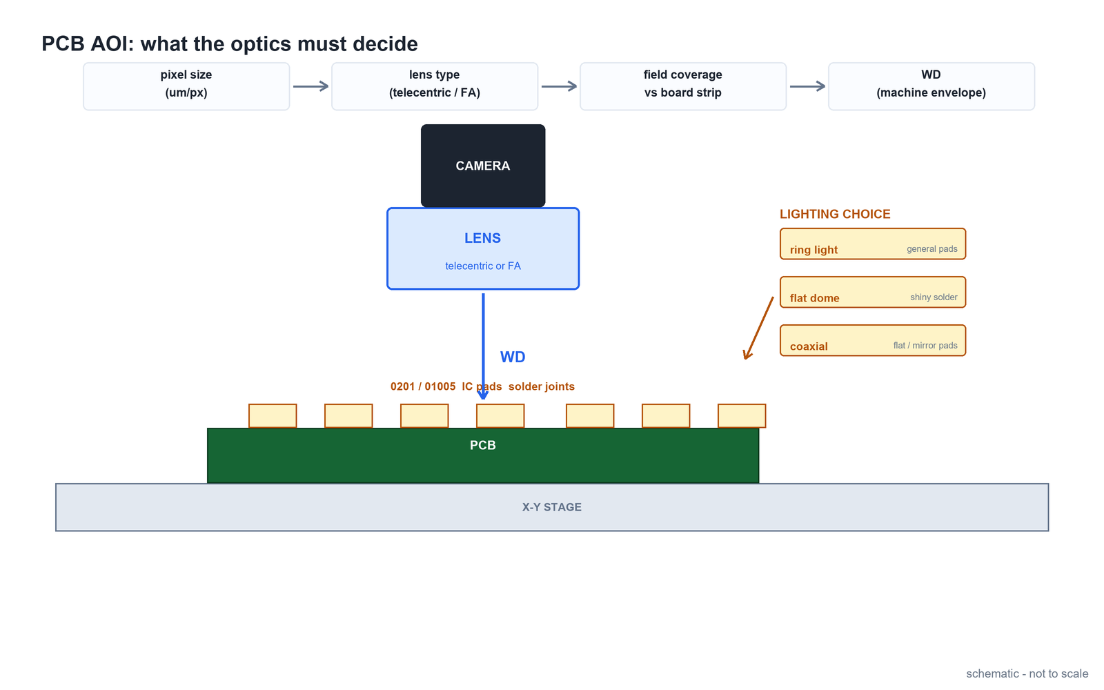
In brief: an AOI station is only as good as the optics in front of the sensor. Four decisions define the optical design: how many micrometres one pixel must cover on the board (pixel size), which lens family matches the board's height variation and accuracy target (telecentric vs FA), how the working distance fits the machine envelope, and which lighting geometry makes solder joints and pads separable. Getting these four in the wrong order produces a system that images the board beautifully and still misses defects.
Part of the POMEAS Machine Vision Optics Selection Guides series — see the Machine Vision Optics Selection Guides index for all 16 articles in this set, grouped by the decision they support.
Step one: pixel size from the smallest feature
Start from the smallest feature that must be reliably detected — for modern boards that is usually the 01005 pad (0.4 × 0.2 mm) or a solder-joint sliver, not the component body. As a common sampling rule, the feature should span at least 3 image points across its critical dimension, which sets a maximum object-space pixel size. In practice AOI stations for fine-pitch work target roughly 20–30 µm per pixel, and accept a coarser figure only when the defect list allows it.
pixel size (µm/px) = FOV width (mm) × 1000 ÷ sensor width (px) — fix the sensor first, then the FOV it can support.
A worked example: a 12 MP camera with a 4096 px wide sensor imaging a 100 mm wide board strip gives 100,000 ÷ 4096 ≈ 24 µm/px. An 01005 pad's 0.2 mm critical dimension then spans about 8 pixels — comfortable for detection, workable for solder-joint judgement.
Step two: lens type against height variation
A PCB is not flat. Components, connectors and finished solder joints create height steps of a few millimetres, and the optics must judge features at several of them in one image.
- Telecentric optics keep magnification stable across that height range and suppress perspective distortion, which matters when the measurement is positional (pad offset, component shift, coplanarity). They cost more, and their field of view is bounded by the lens diameter.
- FA lenses cover large fields cheaply and are the pragmatic choice when the defect list is presence/orientation driven rather than measurement driven — but the magnification drifts with part height and perspective makes offset measurements angle-dependent.
- Motorized zoom optics fit stations that inspect several product families through one camera: magnification changes between recipes without swapping hardware. The magnification-change case for AOI covers that workflow separately.
The choice is a statement about which defects the station owns. Distortion-sensitive positional defects push toward telecentric; coverage-sensitive presence defects tolerate FA; multi-product lines benefit from motorized zoom.
Step three: field coverage versus the stage
Full-board single-shot imaging at 20–30 µm/px demands enormous sensors, which is why most AOI architectures divide the board into strips and rely on a precision X–Y stage. The optical consequence: every strip image must hold its pixel size and distortion at the edges, or the stitched board map drifts. This is the point where lens field flatness and telecentricity stop being datasheet decoration and become stitching accuracy.
Step four: working distance as a machine budget
The WD must clear the conveyour rails, the top lighting and any thickness variation of the panel stack — and the lens must hold its rated geometry at that distance. Long-WD telecentric designs keep the measurement geometry when the machine cannot sit close to the board; a shorter WD buys a smaller, cheaper optical package wherever the envelope allows it.
Lighting: the half of the optics that has no datasheet number
- Ring light — the generalist for pads and silkscreen; fast, cheap, tolerant.
- Flat dome — diffuses specular reflection off shiny solder and IC bodies; the default when joints wash out.
- Coaxial — delivers light down the optical axis for flat, mirror-like pads; pairs naturally with telecentric optics, as covered in the coaxial selection guide.
Solder is the hard surface: it is specular, curved and moving through reflow phases. Most "the camera cannot see the joint" complaints are lighting-geometry complaints, not resolution complaints.
A worked selection, end to end
- Defect list: 01005 presence, polarity, pad offset. → pixel size target ≈ 25 µm/px.
- Sensor: 4096 × 3000, 3.45 µm pixels (14.1 mm wide). → strip FOV ≈ 105 × 77 mm, and the magnification follows: 14.1 ÷ 105 ≈ 0.135X.
- Height variation: connectors 4 mm above board. → DOF and telecentric range must cover ±2 mm or the high features defocus.
- Machine envelope: 65 mm clearance above the tallest panel. → rated WD ≥ 65 mm.
- Lighting: flat dome for joints + coaxial channel for pad-offset measurement.
Every number here came from the defect list, the sensor and the machine — none from the lens catalogue. The catalogue is consulted last, not first.
Frequently asked questions
What pixel size do I need to inspect 01005 components?
Work backwards from the 0.2 mm critical dimension of an 01005 pad: with the common rule of at least 3 image points across the feature, the object-space pixel size must be smaller than roughly 65 µm/px, and fine-pitch AOI stations typically target 20 to 30 µm per pixel so that solder-joint judgement stays possible, not just presence detection.
Should I use a telecentric lens or a standard FA lens for AOI?
Use telecentric optics when the station must measure position across varying component heights, because magnification stability and distortion control decide the result there. A standard FA lens is the pragmatic choice when the defect list is dominated by presence and orientation over a large field and the budget is fixed. Many lines end up mixing both, one camera each.
Why do solder joints look washed out in my images?
Solder is specular and curved, so a fixed illumination angle reflects away from the sensor and the joint loses contrast. Changing the lighting geometry — a flat dome to diffuse the reflection, or a coaxial channel for flat pads — usually restores the contrast that no amount of resolution can substitute for.
Can one camera cover the whole PCB in a single image?
Only at a pixel size too coarse for fine-pitch defects: covering a 300 mm board at 25 µm/px requires a 12000 px sensor just in one direction, and the optics behind it grow accordingly. That is why production AOI divides the board into strips on a precision stage and stitches the map, which keeps the pixel size fixed and the distortion per strip small.
Related products and reading
- Object-side resolution vs measurement accuracy FAQ — why pixel size is necessary but not sufficient for accuracy.
- Motorized zoom lens for AOI: magnification change without downtime — the multi-product workflow.
- Telecentric lens and coaxial illumination selection guide — the optical pair behind pad-offset measurement.
- AOI vision inspection — integrated inspection systems engineered around the decisions above.
- Industrial lenses — FA and telecentric families for strip imaging.
- Machine vision accessories — lighting and cameras that complete the chain.

Subscribe to Our Newsletter
Simply enter your email to receive the latest news and insights from Pomeas. Stay connected with Pomeas and be the first to discover new innovations in optical excellence.